Please refer to Semiconductor Electronics Materials Devices and Simple Circuits MCQ Questions Class 12 Physics below. These MCQ questions for Class 12 Physics with answers have been designed as per the latest NCERT, CBSE books, and syllabus issued for the current academic year. These objective questions for Semiconductor Electronics Materials Devices and Simple Circuits will help you to prepare for the exams and get more marks.
Semiconductor Electronics Materials Devices and Simple Circuits MCQ Questions Class 12 Physics
Please see solved MCQ Questions for Semiconductor Electronics Materials Devices and Simple Circuits in Class 12 Physics. All questions and answers have been prepared by expert faculty of standard 12 based on the latest examination guidelines.
MCQ Questions Class 12 Physics Semiconductor Electronics Materials Devices and Simple Circuits
Question. For an electronic valve, the plate current I and plate voltage V in the space charge limited region are related as
(a) I is proportional to V 3/2
(b) I is proportional to V 2/3
(c) I is proportional to V
(d) I is proportional to V 2
Answer
A
Question. Choose the only false statement from the following.
(a) In conductors the valence and conduction bands overlap.
(b) Substances with energy gap of the order of 10 eV are insulators.
(c) The resistivity of a semiconductor increases with increase in temperature.
(d) The conductivity of a semiconductor increases with increase in temperature.
Answer
C
Question. When using a triode, as an amplifier, the electrons Dare emitted by
(a) grid and collected by cathode only
(b) cathode and collected by the anode only
(c) anode and collected by cathode only
(d) anode and collected by the grid and by cathode.
Answer
B
Question. Carbon, silicon and germanium atoms have four valence electrons each. Their valence and conduction bands are separated by energy band gaps represented by (Eg)C, (Eg)Si and (Eg)Ge respectively. Which one of the following relationships is true in their case?
(a) (Eg)C > (Eg)Si
(b) (Eg)C < (Eg)Si
(c) (Eg)C = (Eg)Si
(d) (Eg)C < (Eg)Ge
Answer
A
Question. The device that can act as a complete electronic circuit is
(a) junction diode
(b) integrated circuit
(c) junction transistor
(d) zener diode.
Answer
B
Question. In semiconductors at a room temperature
(a) the valence band is partially empty and the conduction band is partially filled
(b) the valence band is completely filled and the conduction band is partially filled
(c) the valence band is completely filled
(d) the conduction band is completely empty.
Answer
A
Question. C and Si both have same lattice structure; having 4 bonding electrons in each. However, C is insulator whereas Si is intrinsic semiconductor. This is because
(a) in case of C the valence band is not completely filled at absolute zero temperature
(b) in case of C the conduction band is partly filled even at absolute zero temperature
(c) the four bonding electrons in the case of C lie in the second orbit, whereas in the case of Si they lie in the third
(d) the four bonding electrons in the case of C lie in the third orbit, whereas for Si they lie in the fourth orbit.
Answer
C
Question. When a triode is used as an amplifier the phase difference between the input signal voltage and the output is
(a) 0
(b) p
(c) p/2
(d) p/4.
Answer
B
Question. At absolute zero, Si acts as
(a) non metal
(b) metal
(c) insulator
(d) none of these.
Answer
C
Question. For amplification by a triode, the signal to be amplified is given to
(a) the cathode
(b) the grid
(c) the glass envelope
(d) the anode
Answer
B
Question. For a p-type semiconductor, which of the following statements is true?
(a) Electrons are the majority carriers and pentavalent atoms are the dopants.
(b) Electrons are the majority carriers and trivalent atoms are the dopants.
(c) Holes are the majority carriers and trivalent atoms are the dopants.
(d) Holes are the majority carriers and pentavalent atoms are the dopants.
Answer
C
Question. If a small amount of antimony is added to germanium crystal
(a) it becomes a p-type semiconductor
(b) the antimony becomes an acceptor atom
(c) there will be more free electrons than holes in the semiconductor
(d) its resistance is increased.
Answer
C
Question. Pure Si at 500 K has equal number of electron (ne) and hole (nh) concentrations of 1.5 × 10¹⁶ m–3. Doping by indium increases nh to 4.5 × 10²² m–3. The doped semiconductor is of
(a) p-type having electron concentration ne = 5 × 10⁹ m–3
(b) n-type with electron concentration ne = 5 × 10²² m–3
(c) p-type with electron concentration ne = 2.5 × 10¹⁰ m–3
(d) n-type with electron concentration ne = 2.5 × 10²³ m–3
Answer
A
Question. Which one of the following statement is false?
(a) Pure Si doped with trivalent impurities gives a p-type semiconductor.
(b) Majority carriers in a n-type semiconductor are holes.
(c) Minority carriers in a p-type semiconductor are electrons.
(d) The resistance of intrinsic semiconductor decreases with increase of temperature.
Answer
B
Question. In the energy band diagram of a material shown here, the open circles and filled circles denote holes and electrons respectively. The material is
(a) an insulator
(b) a metal
(c) an n-type semiconductor
(d) a p-type semiconductor.
Answer
D
Question. In a n-type semiconductor, which of the following statement is true?
(a) Holes are minority carriers and pentavalent atoms are dopants.
(b) Holes are majority carriers and trivalent atoms are dopants.
(c) Electrons are majority carriers and trivalent atoms are dopants.
(d) Electrons are minority carriers and pentavalent atoms are dopants.
Answer
A
Question. In a p type semiconductor, the majority carriers of current are
(a) protons
(b) electrons
(c) holes
(d) neutrons
Answer
C
Question. Which of the following, when added as an impurity into the silicon produces n type semiconductor?
(a) B
(b) Al
(c) P
(d) Mg
Answer
C
Question. To obtain a p-type germanium semiconductor, it must be doped with
(a) indium
(b) phosphorus
(c) arsenic
(d) antimony.
Answer
A
Question. When arsenic is added as an impurity to silicon, the resulting material is
(a) n-type conductor
(b) n-type semiconductor
(c) p-type semiconductor
(d) none of these.
Answer
B
Question. The barrier potential of a p-n junction depends on
(1) type of semiconductor material
(2) amount of doping
(3) temperature
Which one of the following is correct?
(a) (1) and (2) only
(b) (2) only
(c) (2) and (3) only
(d) (1), (2) and (3)
Answer
D
Question. In an unbiased p-n junction, holes diffuse from the p-region to n-region because of
(a) he attraction of free electrons of n-region
(b) the higher hole concentration in p-region than that in n-region
(c) the higher concentration of electrons in the n-region than that in the p-region
(d) the potential difference across the p-n junction.
Answer
B
Question. In a p-n junction
(a) high potential at n side and low potential at p side
(b) high potential at p side and low potential at n side
(c) p and n both are at same potential
(d) undetermined.
Answer
A
Question. When n type semiconductor is heated
(a) number of electrons increases while that of holes decreases
(b) number of holes increases while that of electrons decreases
(c) number of electrons and holes remain same
(d) number of electrons and holes increases equally.
Answer
D
Question. The increase in the width of the depletion region in a p-n junction diode is due to
(a) forward bias only
(b) reverse bias only
(c) both forward bias and reverse bias
(d) increase in forward current
Answer
B
Question. Depletion layer consists of
(a) mobile ions
(b) protons
(c) electrons
(d) immobile ions
Answer
D
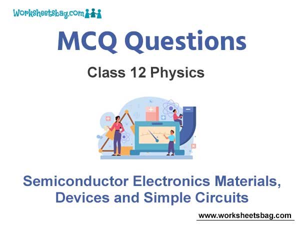
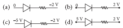
Question. Which one of the following represents forward bias diode?
Answer
D
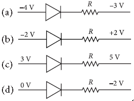
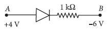
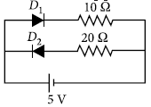
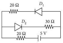
Question. The given circuit has two ideal diodes connected as shown in the figure. The current flowing through the resistance R1 will be
(a) 2.5 A
(b) 10.0 A
(c) 1.43 A
(d) 3.13 A
Answer
A
Question. In a p-n junction diode, change in temperature due to heating
(a) affects only reverse resistance
(b) affects only forward resistance
(c) does not affect resistance of p-n junction
(d) affects the overall V – I characteristics of p-n junction.
Answer
D
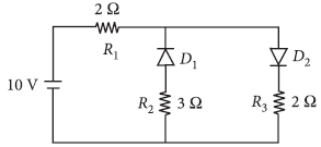
Question. In the given figure, a diode D is connected to an external resistance R = 100 Ω and an e.m.f. of 3.5 V. If the barrier potential developed across the diode is 0.5 V, the current in the circuit will be
(a) 20 mA
(b) 35 mA
(c) 30 mA
(d) 40 mA
Answer
C
Question. In forward biasing of the p-n junction
(a) the positive terminal of the battery is connected to p-side and the depletion region becomes thick.
(b) the positive terminal of the battery is connected to n-side and the depletion region becomes thin.
(c) the positive terminal of the battery is connected to n-side and the depletion region becomes thick.
(d) the positive terminal of the battery is connected to p-side and the depletion region becomes thin.
Answer
D
Question. In the following figure, the diodes which are forward biased, are

(a) (A), (B) and (D)
(b) (C) only
(c) (C) and (A) (d)
(B) and (D)
Answer
C
Question. Consider the junction diode as ideal. The value of current flowing through AB is
(a) 10–1 A
(b) 10–3 A
(c) 0 A
(d) 10–2 A
Answer
D
Question. The depletion layer in the p-n junction region is caused by
(a) drift of holes
(b) diffusion of charge carriers
(c) migration of impurity ions
(d) drift of electrons.
Answer
B
Question. Application of a forward bias to a p-n junction
(a) widens the depletion zone
(b) increases the potential difference across the depletion zone
(c) increases the number of donors on the n side
(d) decreases the electric field in the depletion zone.
Answer
D
Question. If in a p–n junction, a square input signal of 10 V is applied, as shown,
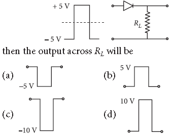
Answer
B
Question. The following figure shows a logic gate circuit with two inputs A and B and the output Y. The voltage waveforms of A, B and Y are as given.
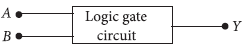
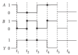
The logic gate is
(a) NOR gate
(b) OR gate
(c) AND gate
(d) NAND gate
Answer
D
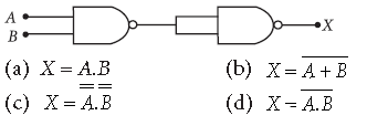
Question. The symbolic representation of four logic gates are given here
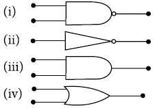
Answer
B
Question. Two ideal diodes are connected to a battery as shown in the circuit. The current supplied by the battery is
(a) 0.75 A
(b) zero
(c) 0.25 A
(d) 0.5 A
Answer
D
Question. For the given circuit of p-n junction diode which is correct?
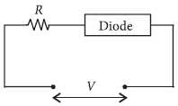
(a) In forward bias the voltage across R is V.
(b) In reverse bias the voltage across R is V.
(c) In forward bias the voltage across R is 2V.
(d) In reverse bias the voltage across R is 2V.
Answer
A
Question. Of the diodes shown in the following diagrams, which one is reverse biased ?
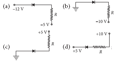
Answer
C
Question. The current in the circuit will be
(a) 5/40 A
(b) 5/50 A
(c) 5/10 A
(d) 5/20 A
Answer
B
Question. Reverse bias applied to a junction diode
(a) lowers the potential barrier
(b) raises the potential barrier
(c) increases the majority carrier current
(d) increases the minority carrier current
Answer
B
Question. From the following diode circuit, which diode is in forward biased condition
Answer
A
Question.. In forward bias, the width of potential barrier in a p-n junction diode
(a) remains constant
(b) decreases
(c) increases
(d) first (a) then (b)
Answer
B
Question. A semiconducting device is connected in a series circuit with a battery and a resistance. A current is found to pass through the circuit. If the polarity of the battery is reversed, the current drops to almost zero. The device may be
(a) a p-type semiconductor
(b) an intrinsic semiconductor
(c) a p-n junction
(d) an n-type semiconductor
Answer
C
Question. Barrier potential of a p-n junction diode does not depend on
(a) diode design
(b) temperature
(c) forward bias
(d) doping density
Answer
A
Question. The diode used in the circuit shown in the figure has a constant voltage drop at 0.5 V at all currents and a maximum power rating of 100 milli watts. What should be the value of the resistor R, connected in series with diode for obtaining maximum current?
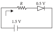
(a) 6.76 W
(b) 20 W
(c) 5 W
(d) 5.6 W.
Answer
C
Question. In the case of forward biasing of p-n junction, which one of the following figures correctly depicts the direction of flow of carriers?

Answer
B
Question. In a junction diode, the holes are due to
(a) extra electrons
(b) neutrons
(c) protons
(d) missing of electrons
Answer
D
Question. The peak voltage in the output of a half wave diode rectifier fed with a sinusoidal signal without filter is 10 V. The d.c. component of the output voltage is
(a) 10 / 2 V
(b) 10/p V
(c) 10 V
(d) 20/p V
Answer
B
Question. An LED is constructed from a p-n junction diode using GaAsP. The energy gap is 1.9 eV. The wavelength of the light emitted will be equal to
(a) 10.4 × 10⁻²⁶ m
(b) 654 nm
(c) 654 Å
(d) 654 × 10–11 m
Answer
B
Question. The given graph represents V-I characteristic for a semiconductor device. Which of the following statement is correct?
(a) It is V-I characteristic for solar cell where, point A represents open circuit voltage and point B short circuit current.
(b) It is for a solar cell and points A and B represent open circuit voltage and current, respectively.
(c) It is for a photodiode and points A and B represent open circuit voltage and current, respectively.
(d) It is for a LED and points A and B represent open circuit voltage and short circuit current, respectively.
Answer
A
Question. The cause of the potential barrier in a p-n junction diode is
(a) depletion of negative charges near the junction
(b) concentration of positive charges near the junction
(c) depletion of positive charges near the junction
(d) concentration of positive and negative charges near the junction.
Answer
D
Question. A Zener diode, having breakdown voltage equal to 15V, is used in a voltage regulator circuit shown in figure. The current through the diode is
(a) 5 mA
(b) 10 mA
(c) 15 mA
(d) 20 mA
Answer
A
Question. A p-n photodiode is fabricated from a semiconductor with a band gap of 2.5 eV. It can detect a signal of wavelength
(a) 4000 nm
(b) 6000 nm
(c) 4000 Å
(d) 6000 Å
Answer
C
Question. If a full wave rectifier circuit is operating from 50 Hz mains, the fundamental frequency in the ripple will be
(a) 25 Hz
(b) 50 Hz
(c) 70.7 Hz
(d) 100 Hz
Answer
D
Question. A p-n junction diode can be used as
(a) condenser
(b) regulator
(c) amplifier
(d) rectifier
Answer
D
Question. Zener diode is used for
(a) amplification
(b) rectification
(c) stabilisation
(d) producing oscillations in an oscillator.
Answer
C
Question. A p-n photodiode is made of a material with a band gap of 2.0 eV. The minimum frequency of the radiation that can be absorbed by the material is nearly
(a) 1 × 10¹⁴ Hz
(b) 20 × 1014 Hz
(c) 10 × 1014 Hz
(d) 5 × 10¹⁴ Hz
Answer
D
Question. In a p-n junction photo cell, the value of the photoelectromotive force produced by monochromatic light is proportional to
(a) the barrier voltage at the p-n junction
(b) the intensity of the light falling on the cell
(c) the frequency of the light falling on the cell
(d) the voltage applied at the p-n junction.
Answer
B
Question. For the logic circuit shown, the truth table is
Answer
A
Question. The correct Boolean operation represented by the circuit diagram drawn is
(a) NOR
(b) AND
(c) OR
(d) NAND
Answer
D
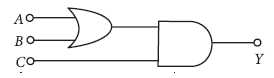
Question. What is the output Y in the following circuit, when all the three inputs A, B, C are first 0 and then 1 ?

(a) 0, 1
(b) 0, 0
(c) 1, 0
(d) 1, 1
Answer
C
Question. The output (X) of the logic circuit shown in figure will be
Answer
A
Question. The output from of a NAND gate is divided into two in parallel and fed to another NAND gate. The resulting gate is a

(a) AND gate
(b) NOR gate
(c) OR gate
(d) NOT gate
Answer
A
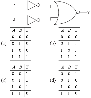
Question. In the combination of the following gates the output Y can be written in terms of inputs A and B as

Answer
B
Question. The given electrical network is equivalent to

(a) OR gate
(b) NOR gate
(c) NOT gate
(d) AND gate
Answer
B
Question. The figure shows a logic circuit with two inputs A and B and the output C. The voltage wave forms across A, B and C are as given. The logic circuit gate is
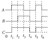
(a) OR gate
(b) NOR gate
(c) AND gate
(d) NAND gate
Answer
A
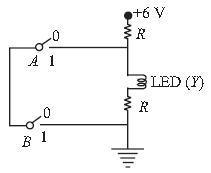
Question. To get output 1 for the following circuit, the correct choice for the input is
(a) A = 1, B = 1, C = 0
(b) A = 1, B = 0, C = 1
(c) A = 0, B = 1, C = 0
(d) A = 1, B = 0, C = 0
Answer
B
Question. Symbolic representation of four logic gates are shown as Pick out which ones are for AND, NAND and NOT gates, respectively
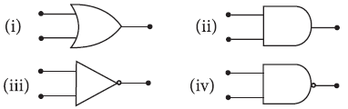
(a) (ii), (iii) and (iv)
(b) (iii), (ii) and (i)
(c) (iii), (ii) and (iv)
(d) (ii), (iv) and (iii)
Answer
D