Students should refer to Worksheets Class 12 Physics Semiconductor Electronics: Materials, Devices and Simple Circuits Chapter 14 provided below with important questions and answers. These important questions with solutions for Chapter 14 Semiconductor Electronics: Materials, Devices and Simple Circuits have been prepared by expert teachers for Class 12 Physics based on the expected pattern of questions in the Class 12 exams. We have provided Worksheets for Class 12 Physics for all chapters on our website. You should carefully learn all the important examinations questions provided below as they will help you to get better marks in your class tests and exams.
Semiconductor Electronics: Materials, Devices and Simple Circuits Worksheets Class 12 Physics
Question: A potential barrier of 0.3 V exists across a p-n junction. If the depletion region is 1 mm wide, what is the intensity of electric field in this region?
(a) 2 × 10⁵ V m–1
(b) 3 × 10⁵ V m–1
(c) 4 × 10⁵ V m–1
(d) 5 × 10⁵ V m–1
Answer:
B
Question: Which of the following statements is correct?
(a) Hole is an antiparticle of electron.
(b) Hole is a vacancy created when an electron leaves a covalent bond.
(c) Hole is the absence of free electrons.
(d) Hole is an artificially created particle.
Answer:
B
Question: The equivalent resistance of the circuit shown in figure between the points A and B if VA < VB is
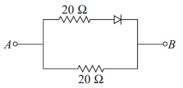
(a) 10Ω
(b) 20Ω
(c) 5Ω
(d) 40Ω
Answer:
B
Question: In an unbiased p-n junction, holes diffuse from the p-region to n-region because
(a) free electrons in the n-region attract them
(b) they move across the junction by the potential difference
(c) hole concentration in p-region is more as compared to n-region
(d) all of these.
Answer:
C
Question: When the voltage drop across a p-n junction diode is increased from 0.65 V to 0.70 V, the change in the diode current is 5 mA. The dynamic resistance of the diode is
(a) 20 Ω
(b) 50Ω
(c) 10 Ω
(d) 80 Ω
Answer:
C
Question: If a small amount of antimony is added to germanium crystal
(a) its resistance is increased
(b) it becomes a p-type semiconductor
(c) there will be more free electrons than holes
in the semiconductor
(d) none of these.
Answer:
C
Question: Which of the junction diodes shown below are forward biased?
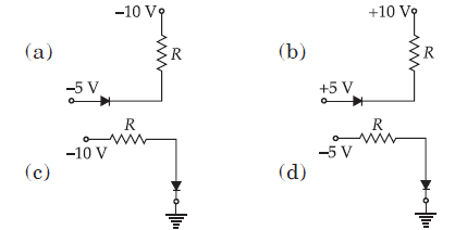
Answer:
A
Question: A sinusoidal voltage of rms value 220 V is applied to a diode and a resistor R in the circuit shown in figure, so that half wave rectification occurs. If the diode is ideal, what is the rms voltage across R1?
(a) 55√ 2 V
(b) 110 V
(c) 110 √2 V
(d) 220 √2 V
Answer:
C
Question: Which of the following statements is incorrect for the depletion region of a diode?
(a) There are mobile charges exist.
(b) Equal number of holes and electrons exist, making the region neutral.
(c) Recombination of holes and electrons has taken place.
(d) None of these.
Answer:
A
Question: If the energy of a proton of sodium light (λ = 589 nm) equals the band gap of semiconductor, the minimum energy required to create hole electron pair
(a) 1.1 eV
(b) 2.1 eV
(c) 3.2 eV
(d) 1.5 eV
Answer:
B
Question: Which of the following circuits provides full wave rectification of an ac input?
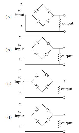
Answer:
D
Question: The circuit shown in the figure contains two diodes each with a forward resistance of 30 W and with infinite backward resistance. If the battery is 3 V, the current through the 50 W resistance (in ampere) is
(a) zero
(b) 0.01
(c) 0.02
(d) 0.03
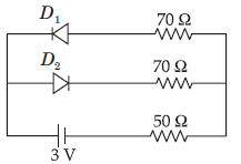
Answer:
C
Question: Carbon, silicon and germanium have four valence electrons each. These are characterised by valence and conduction bands separated by energy band gap respectively equal to (Eg)C, (Eg)Si and (Eg)Ge.Which of the following statements is true?
(a) (Eg)Si < (Eg)Ge < (Eg)C
(b) (Eg)C < (Eg)Ge < (Eg)Si
(c) (Eg)C > (Eg)Si > (Eg)Ge
(d) (Eg)C = (Eg)Si = (Eg)Ge
Answer:
C
Question: Which of the following equations correctly represents the temperature variation of energy gap between the conduction and valence bands for Si?
(a) Eg(T) = 0.70 – 2.23 × 10⁻⁴T eV
(b) Eg(T) = 0.70 + 2.23 × 10⁻⁴T eV
(c) Eg(T) = 1.10 – 3.60 × 10⁻⁴T eV
(d) Eg(T) = 1.10 + 3.60 × 10⁻⁴T eV
Answer:
C
Question: The maximum wavelength of electromagnetic radiation, which can create a hole-electron pair in germanium. (Given that forbidden energy gap in germanium is 0.72 eV)
(a) 1.7 × 10⁻⁶ m
(b) 1.5 × 10⁻⁵ m
(c) 1.3 × 10⁻⁴ m
(d) 1.9 × 10⁻⁵ m
Answer:
A
Question: The dominant mechanism for motion of charge carriers in forward and reverse biased silicon p-n junction are
(a) drift in forward bias, diffusion in reverse bias
(b) diffusion in forward bias, drift in reverse bias
(c) diffusion in both forward and reverse bias
(d) drift in both forward and reverse bias.
Answer:
B
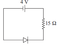
Question: In the circuit shown if drift current for the diode is 20 mA, the potential difference across the diode is
(a) 2 V
(b) 4.5 V
(c) 4 V
(d) 2.5 V
Answer:
C
Question: A potential barrier of 0.50 V exists in a p-n junction. If the depletion region is 5.0 × 10⁻⁷ m thick, what is the electric field in this region?
(a) 1 × 10³ V m–1
(b) 1.0 × 10⁶ V m–1
(c) 1 × 10² V m–1
(d) 1 × 10⁴ V m–1
Answer:
B
Case Based MCQs
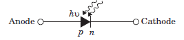
Photodiode
A photodiode is an optoelectronic device in which current carriers are generated by photons through photo-excitation i.e., photoconduction by light. It is a p-n junction fabricated from a photosensitive semiconductor and provided with a transparent window so as to allow light to fall on its junction. A photodiode can turn its current ON and OFF in nanoseconds. So, it can be used as a fastest photo-detector.
Question: Photodiode is a device
(a) which is always operated in reverse bias.
(b) which is always operated in forward bias.
(c) in which photocurrent is independent of intensity of incident radiation.
(d) which may be operated in both forward or reverse bias.
Answer:
A
Question: To detect light of wavelength 500 nm, the photodiode must be fabricated from a semiconductor of minimum bandwidth of
(a) 1.24 eV
(b) 0.62 eV
(c) 2.48 eV
(d) 3.2 eV
Answer:
C
Question: Photodiode can be used as a photodetector to detect
(a) optical signals
(b) electrical signals
(c) both (a) and
(b) (d) none of these.
Answer:
A
Potential Barrier
The potential barrier in the p-n junction diode is the barrier in which the charge requires additional force for crossing the region. In other words, the barrier in which the charge carrier stopped by the obstructive force is known as the potential ba rrier.
When a p-type semiconduct or is brought into a close contact with n-type semiconductor, we get a p-n junction with a barrier potential of 0.4 V and width of depletion region is 4.0 × 10⁻⁷ m.
This p-n junction is forward biased with a battery of voltage 3 V and negligible internal resistance, in series with a resistor of resistance R, ideal millimeter and key K as shown in figure.
When key is pressed, a current of 20 mA passes through the diode.

Question: The intensity of the electric field in the depletion region when p-n junction is unbiased is
(a) 0.5 × 10⁶ V m–1
(b) 1.0 × 10⁶ V m–1
(c) 2.0 × 10⁶ V m–1
(d) 1.5 × 10⁶ V m–1
Answer:
B
Question: The resistance of resistor R is
(a) 150 Ω
(b) 300 Ω
(c) 130 Ω
(d) 180 Ω
Answer:
C
Question: If the voltage of the potential barrier is V0. A voltage V is applied to the input, at what moment will the barrier disappear?
(a) V < V0
(b) V = V0
(c) V > V0
(d) V << V0
Answer:
B
Question: If an electron with speed 4.0 × 10⁵ m s–1 approaches the p-n junction from the n-side, the speed with which it will enter the p-side is
(a) 1.39 × 10⁵ m s–1
(b) 2.78 × 10⁵ m s–1
(c) 1.39 × 10⁶ m s–1
(d) 2.78 × 10⁶ m s–1
Answer:
A
Very Short Answer Type Questions
Question: Why cannot we use Si and Ge in fabrication of visible LEDs?
Answer: LED’s must have band gap in the order of 1.8 eV to 3 eV but Si and Ge have band gap less than 1.8 eV.
Question: Can the potential barrier across a p-n junction be measured by simply connecting a voltmeter across the junction?
Answer: No, the voltmeter should have a very high resistance as compared to the resistance of p-n junction, which is nearly infinite.
Question: How does an increase in doping concentration affect the width of depletion layer of a p-n junction diode?
Answer: When there is an increase in doping concentration, the applied potential difference causes an electric field which acts opposite to the potential barrier. This results in reducing the potential barrier and hence the width of depletion layer decreases.
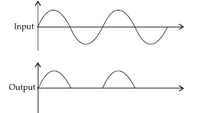
Question: Draw the output waveform across the resistor.
Answer: The diode acts as half wave rectifier, it offers low resistance when forward biased and high resistance when reverse biased.
Short Answer Type Questions
Question: What is the current flowing in R2 in the circuit shown in figure? Given : R1 = 500 W and R2 = 1 k Ω

Answer: The diode is reverse biased, but the voltage across it is given as 5 V. R2 is in parallel with the diode, so current in R2 = 5V/1000Ω ⇒ Current in R2 = 5 mA.
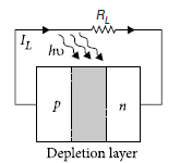
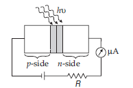
Question: With the help of a simple diagram, explain the working of a silicon solar cell giving all three basic processes involved.
Answer: Principle : A solar cell works on the principle of photovoltaic effect according to which when light photons of energy greater than energy band gap of a semiconductor are incident on p-n junction of that semiconductor, electron-hole pairs are generated which give rise to an emf.
Generation of emf : Three basic processes are involved in the generation of emf by a solar cell when solar radiations are incident on it. These are:
(i) The generation of electron-hole pairs close to the junction due to incidence of light with photo energy hu ≥ Eb.
(ii) The separation of electrons and holes due to the electric field of the depletion region. So, electrons are swept to n-side and holes to p-side.
(iii) The electrons reaching the n-side are collected by the front contact and holes reaching p-side are collected by the back contact.
Thus, p-side becomes positive and n-side become negative giving rise to a photovoltage.
When an external load RL is connected as shown in figure, a photocurrent IL begins to flow through the load.
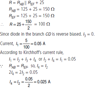
Question: If each diode in figure has a forward bias resistance of 25 Ω and infinite resistance in reverse bias, what will be the values of the current I1, I2, I3 and I4?
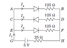
Answer: Let R be the effective resistance of the circuit, then
Question: (a) Distinguish between n-type and p-type semiconductors on the basis of energy band diagrams.
(b) Compare their conductivities at absolute zero temperature and at room temperature.
Answer: (a) The required energy band diagrams are given below:
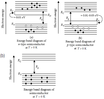
At absolute zero temperature (0 K), conduction band of semiconductor is completely empty, i.e., s = 0. Hence the semiconductor behaves as an insulator. At room temperature, some valence electrons acquire enough thermal energy and jump to the conduction band where they are free to conduct electricity. Thus the semiconductor acquires a all conductivity at room temperature.
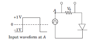
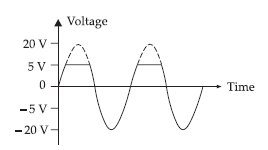
Question: Direction : Read the following and answer the questions given below.
Light emitting diode is a photoelectric device which converts electrical energy into light energy. It is a heavily doped p-n junction diode which under forward biased emits spontaneous radiation. The general shape of the I-V characteristics of an LED is similar to that of a normal p-n junction diode, as shown. The barrier potentials are much higher and slightly different for each colour.

(i) Draw the I-V characteristic of an LED.
(ii) Draw the schematic symbol of light emitting diode (LED).
(iii) An LED is constructed from a p-n junction based on a certain Ga-As-P semiconducting material whose energy gap is 1.9 eV. Identify the colour of the emitted light.
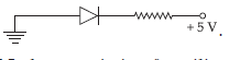
(iv) Assuming the ideal diode, draw the output waveform for the circuit given in figure. Explain the waveform.
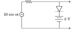
Answer: (i) The I-V characteristics of an LED is similar to that of a Si junction diode. But the threshold voltages are much higher and slightly different for each colour.


(iv) For the voltage less than 5 V, the diode is reverse biased and circuit will act as open circuit.
When input voltage is greater than 5 V, diode is in conducting state.
Question: Suppose a ‘n’-type wafer is created by doping Si crystal having 5 × 1028 atoms/m3 with 1 ppm concentration of As. On the surface 200 ppm Boron is added to create ‘p’ region in this wafer. Considering ni = 1.5 × 10¹⁶ m–3,
(a) Calculate the densities of the charge carriers in the n and p regions.
(b) Comment which charge carriers would contribute largely for the reverse saturation current when diode is reverse biased.
Answer:

(b) The minority carrier holes of n-region wafer (nh = 0.45 × 10¹⁰ m–3) would contribute more to reverse saturation current than minority carrier electrons of p–region wafer (ne = 2.25 × 10⁷ m–3) when p – n junction is reverse biased.
Question: In the following diagram ‘S’ is a semiconductor.
Would you increase or decrease the value of R to keep the reading of the ammeter A constant when S is heated? Give reason for your answer.

Answer: We will increase the value of R. On heating a semiconductor, its resistance decreases with rise in temperature. As the semiconductor, S is in series, so net resistance of the circuit also decreases. So by increasing the value of R we can keep the resistance of circuit constant and hence the current in the circuit or the reading of ammeter A can be kept constant.
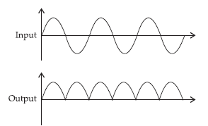
Question: In half-wave rectification, what is the output frequency if the input frequency is 50 Hz. What is the output frequency of a full-wave-rectifier for the same input frequency?
Answer: In half wave rectification, only one ripple is obtained per cycle in the output.
Output frequency of a half wave rectifier = input frequency = 50 Hz
In full wave rectification, two ripples are obtained per cycle in the output.
Output frequency = 2 × input frequency = 2 × 50 = 100 Hz
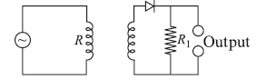
Question: Explain, with the help of a circuit diagram, the working of a photodiode. Write briefly how it is used to detect the optical signals.
Answer: Working of photodiode :
A junction diode made from light sensitive semiconductor is called a photodiode. A photodiode is a p-n junction diode arranged in reverse biasing.
The number of charge carriers increases when light of suitable frequency is made to fall on the p-n junction, because new electron-hole pairs are created by absorbing the photons of suitable frequency. Intensity of light controls the number of charge carriers. Due to this property photodiodes are used to detect optical signals.
Question: In the case of n-type Si-semiconductor, the donor energy level is slightly below the bottom of conduction band whereas in p-type semiconductor, the acceptor energy level is slightly above the top of valence band. Explain, giving examples, what role do these energy levels play in conduction and valence bands.
Answer: In n-type extrinsic semiconductors, the number of free electrons in conduction band is much more than the number of holes in valence band. The donor energy level lies just below the conduction band. In p-type extrinsic semiconductor, the number of holes in valence band is much more than the number of free electrons in conduction band. The acceptor energy level lies just above the valence band.
Question: (a) Why are Si and GaAs preferred materials for fabrication in solar cells?
(b) Draw V-I characteristic of solar cell and mention its significance.
Answer: (a) The energy for the maximum intensity of the solar radiation is nearly 1.5 eV. In order to have photo excitation the energy of radiation (hu) must be greater than energy band gap (Eg), i.e., hu > Eg. Therefore, th e semiconductor with energy band gap about 1.5 eV or lower and with higher absorption coefficient, is likely to give better solar conversion efficiency.
The energy band gap for Si is about 1.1 eV, while for GaAs, it is about 1.53 eV. The gas GaAs is better inspite of its higher bandgap than Si because it absorbs relatively more energy from the incident solar radiations being of relatively higher absorption coefficient.
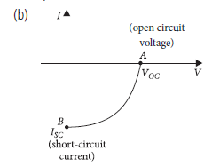
(i) V-I curve is drawn in the fourth quadrant, because a solar cell does not draws current but supply current to the load.
(ii) In V-I curve, the point A indicates the maximum voltage Voc being supplied by the given solar cell when no current is being drawn from it.Voc is called the open circuit voltage (iii) In V-I curve, the point B indicates the maximum current ISC which can be obtained by short circuiting the solar cell without any load resistance. ISC is called the short circuit current.
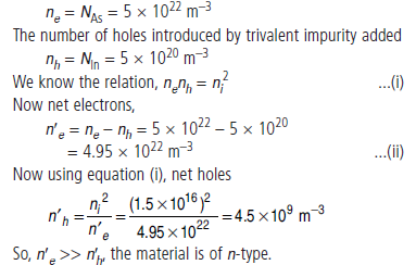
Question: The number of silicon atoms per m3 is 5 × 1028. This is doped simultaneously with 5 × 10²² atoms per m3 of Arsenic and 5 × 10²⁰ per m3 atoms of Indium. Calculate the number of electrons and holes. Given that ni = 1.5 × 10¹⁶ m–3. Is the material n-type or p-type?
Answer: We know that for each atom doped with Arsenic, one free electron is received. Similarly, for each atom doped with indium, a vacancy is created.
So, the number of free electrons introduced by pentavalent impurity added,
Long Answer Type Questions
Question: Draw the circuit arrangement for studying the V-I characteristics of a p-n junction diode in
(i) forward and (ii) reverse bias. Briefly explain how the typical V-I characteristics of a diode are obtained and draw these characteristics.
Answer: Forward biased characteristics : The circuit diagram for studying forward biased characteristics is shown in the figure.
Starting from a low value, forward bias voltage is increased step by step (measured by voltmeter) and forward current is noted (by ammeter). A graph is plotted between voltage and current. The curve so obtained is the forward characteristic of the diode.
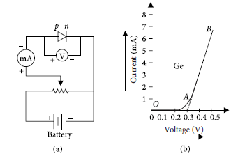
At the start when applied voltage is low, the current through the diode is almost zero. It is because of the potential barrier, which opposes the applied voltage. Till the applied voltage exceeds the potential barrier, the current increases very slowly with increase in applied voltage (OA portion of the graph).
With further increase in applied voltage, the current increases very rapidly (AB portion of the graph), in this situation, the diode behaves like a conductor. The forward voltage beyond which the current through the junction starts increasing rapidly with voltage is called threshold or cut-in voltage. If line AB is extended back, it cuts the voltage axis at potential barrier voltage.
Reverse biased characteristics : The circuit diagram for studying reverse biased characteristics is shown in the figure.
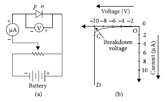
In reverse biased, the applied voltage supports the flow of minority charge carriers across the junction. So, a very small current flows across the junction due to minority charge carriers.
Motion of minority charge carriers is also supported by internal potential barrier, so all the minority carriers cross over the junction.
Therefore, the small reverse current remains almost constant over a sufficiently long range of reverse bias, increasing very little with increasing voltage (OC portion of the graph). This reverse current is voltage independent upto certain voltage known as breakdown voltage and this voltage independent current is called reverse saturation current.
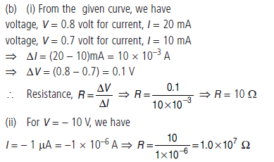
Question:(a) In the following diagram, is the junction diode forward biased or reverse biased?
(b) The V-I characteristic of a silicon diode is as shown in the figure. Calculate the resistance of the diode at (i) I = 15 mA and
(ii) V = –10 V

Answer: (a) Voltage at p side is less than voltage at n side of the diode so it is in reverse bias